Backup RAM data format

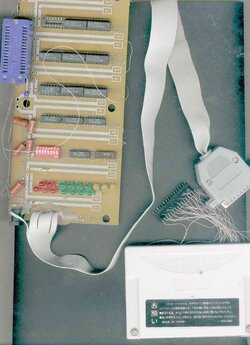
Hi everybody. A few days ago I've finally finished my homebrew Backup RAM reader/writer. So now I can backup/restore RAM image. But processing full RAM can take a lot of time (up to 3-4 minutes) 'cause I haven't optimized software yet (and LPT sucks), and It's kinda uncomfortably backuping/restoring all RAM when I need only 21 blocks....

So does anybody have info about RAM data format? Now the only things i know that block size is 64 bytes, saves are stored in clusters of 4*n blocks (multiple 100h), and damn, saves are scaterred all over the RAM. Save starts at XXX00(hex) with 80 00 00 XX (hex), and if XX is 01, then save is incessant.
 
Hi Jameson!

Cool thing you did, indeed! Some files on official Backup RAM are so big that they don't fit into System Memory. So your Reader/Writer is the only solution to get them off the cartridge.

Could you please post some pictures of it?

I have a lot of cartridges, too. And I tried to get some info out of them like the pinout. I got the voltage supply pins, address and data pins, but as I know from genesis, there are a lot of other usefull signals.

Have you got any information about the pinout? Would help me much!

If you want to know the storage format in backup cartridge, you would have to do it with reenginering.

You could either write or find a saturn program that allows you to read out memory locations while the backup cart is plugged, or you could compare the data you download with your Reader with the gamesaves which you can get via Action Replay onto PC. Note that these gamesaves got 4 zero bytes inserted from time to time.

Thanks,

The Rockin'-B

BTW: the dev central would be a better place for such questions
 
Thanks, Rockin'-B

Actually it's not as cool as You suppose. It's pretty dumb (I mean simple :) ) and pretty ugly, but I'll post a picture if you insist. I can even post schematics if you need it.

The only thing I know about these cartridges is an official datasheet for AT29C040 from Atmel's website.

It's a 4MBit flash IC, and almost every pin comes directly to Saturn's socket, so I simply connected my so-called programmer directly to this IC. The only difference is that instead of IC's Chip Enable (CE) cartridge has 2 pins: latch enable and chip enable controlled via 74 series logics. As you can see from picture, this device contains only DIP32 socket 'cause tests were performed on DIP32 AT29C040 chip. It's too difficult for me to built a Saturn-like socket, so I soldered a DIP32 panel to cartridge directly... And don't be afraid of KP1533NP15 chips (it's not actually N, it's russian I), is'a russian analog of 74HC173. K155, jumpers and resistors aren't used, they're from previous development. If you've got some questions, feel free to ask'em.

I don't have any information about everything else in socket's pinout, but you can find it here(the page is in japanese, but I suppose it's not a problem), in section 17 there is a connector himself, but I haven't traced links yet.

I have alredy started a reenginering process, but I'm still out of data. I have an Action Replay (damn, I lost it somewhere in my room... where can it be....), but I don't have a PC link card, and I suppose it's kinda difficult to find it here in Russia. The only choises is either to order it from USA (it works, but slow), or make it myself :) Just kidding, I'm not good enough to make ISA/PCI devices yet.

Maybe somebody can assist me in this task? I will need only AR save binaries I suppose... If someone is interested, please mail me.
 

Attachments

  • device2.jpg
    device2.jpg
    88.4 KB · Views: 127
  • device2.jpg
    device2.jpg
    88.4 KB · Views: 123
I dunno if this is useful to you or not, but you can use my save game copier to copy a save game file to the saturn's backup memory. You burn the file to cd, and copy.

Another option would be to use one of the Saturn emulators that are out, Satourne and Giri Giri both support backup ram. Copy a file to backup ram, and reverse engineer with a hex editor.
 
Annoyingly, the backup library is one of the components Sega didn't provide the sources from in SBL, but the headers and object files would be one place to start reverse-engineering.

Anyway, if you're looking for Commlinks, I know at least one place here in Finland that carries them.
 
Jameson: can you determine which cart pins provide CE, OE, and WE? I've been looking for this for a little while and would really appreciate any info on it... in the mean time I'll navigate the maze of dummy bus names in those schematics. :)

Just kidding, I'm not good enough to make ISA/PCI devices yet.

The hard part for ISA would be making the edge connector, the circuitry is not that advanced. By the way, you might want to check out Free Wing's parallel port interface for the comms port... the design is not very elegant or fast but it's compatible with SPP and is not too difficult to build.

edit:

Annoyingly, the backup library is one of the components Sega didn't provide the sources from in SBL

That's because it lives in the BIOS.
 
slinga, I think you program can be useful. Wouldn't you mind posting a link?

antime, the main difficulty is that ordering something from USA for me is much easier than even from the neighbour Poland because of our stupid banking system (or should I say its absence?). Thanks for the offer, though.

ExCyber, is there any difficulty? I just disassembled my RAM cart and traced all links with multimeter (actually they use two-layered PCB, so most of the links can be traced visually). I even compiled schematic circuit. Here's info about WE, CE and OE:

First about my pin nubmering system. If you'll look at the cartrige from the front (not upside down), the most left-handed pin will be 1F (front), and the right handed 67F. If you'll look at the back (upside down), left will be 1B and right will be 67B. Gap must be between 36F/36B and 37F/37B. All places with no lamellas are counted too (gap space is not counted).

So, WE is connected to 49B directly, OE is connected to 47F directly, and CE is controlled via 48F and 32B. If 48F is 0V, and 32B is 0V, then CE is active (0V), latch disabled, if 48F is 5V and 32B is 0V then CE is passive (5V), latch disabled, and if 32B is 5V then latch is enabled (any attempt to read will result in receiving 01h byte, and I suppose any attempt to write will write 01h to the specified address). I hope this will be helpful.
 
ExCyber, is there any difficulty? I just disassembled my RAM cart and traced all links with multimeter (actually they use two-layered PCB, so most of the links can be traced visually).

On the cartridge (EMS Action Replay 4M Plus) I have, those signals are decoded by two interconnected PAL chips, so they can't just be traced, I would have had to attach probes or LEDs to the signals and run through address sweeps to isolate the signals... anyway thanks for the information, this is hopefully now enough for me to be able to connect a memory to the A-Bus. :)

if 32B is 5V then latch is enabled (any attempt to read will result in receiving 01h byte, and I suppose any attempt to write will write 01h to the specified address).

I'm not sure what latch you mean. It sounds like there's a 7414 or similar chip providing a locking mechanism for the flash memory, is that correct? Also, I found that my notes only go up to A17, do you have info on any higher address lines? It sounds like 48F is the A-Bus CS0 signal, and 32B is A20. I know in theory I should be able to trace higher address lines from the DRAM, but on this cart they appear to be interleaved in an odd way so I can only identify that they are > A17. This has no effect on the DRAM's functionality since the ordering is the same for both writing and reading... I guess the address pins should go something like:

A18: 33F

A19: 33B

A20: 32B

A21: 32F

A22: 32B

A23: 31F

A24: 30F

But this is really only a guess, can you confirm any of it?

I'm pretty confident that 47B is CS1 (cart ID lives here on most carts), and 48B is most likely CS2 if the numbering is consistent at all, though I'm not sure how useful this would be unless the cart slot has signals for bus mastering, since CS2 is the CS signal for the CD-ROM interface. Now I'm off in search of CAS/RAS...
 
ExCyber, latch used in Sega's RAM cart (both mine and my friend's) is 74244. First input is connected to 5V, remaining - to 0V, outputs - directly to data bus, control inputs (soldered together) - to 48F and 32B via 7400 NAND as I described before. Actually, my EMS's Action Replay uses similar IC (74245) for latching link port. Regrettably my RAM cart doesn't have address lines higher than A18 'cause it's using 2^19 bytes RAM, and I'm not sure if it really coincide with DRAM's. Anyway, here's full pin refference of my cart (according to flash IC address/data bus)

Address line:

A0 45B

A1 44F

A2 43F

A3 42F

A4 40F

A5 39F

A6 38F

A7 40B

A8 42B

A9 44B

A10 43B

A11 38B

A12 39B

A13 37F

A14 37B

A15 35F

A16 35B

A17 34F

A18 34B

Data line:

D0 55B

D1 56B

D2 57B

D3 58B

D4 58F

D5 57F

D6 56F

D7 55F

Sega's RAM cart doesn't have neither 30F-33F nor 31B&33B, 47B&48B are missing too, so I can't confirm your guess. Yeah, you said A20 and A22 are both connected to 32B. Is this a misprint or you mean they're multiplexed ? In first case I suppose A22 must be 31B...

slinga, I've found your program. I'll try to use it.

BTW, I've posted some topic-related materials at my web account. If anyone is

interested, you can check it here
 
Yeah, you said A20 and A22 are both connected to 32B. Is this a misprint or you mean they're multiplexed ? In first case I suppose A22 must be 31B...

Having A20 and A22 connected was a typo. Also, my numbering starts at A1 (because the A-Bus is a 16-bit bus).
 
Back
Top