DMA Transfer

paul_met

Established Member
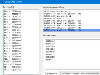
Digging into the resources of a particular game, I often come across the following code (see screenshot). I understand that this is reading / writing using DMA. But I don't fully understand how it works. From what I figured it out:
  • The value in register R4 is the address of data reading (in the this case, reading from CD, but it is not clear from which sector).
  • The value in register R5 is the address for writing data (everything is clear with this).
  • The value in register R6 is the size of the data block that will be read and written (using 32 bits value, so the data size is divisible by 4).
  • The value in register R7 is some kind of bus usage identifier (I didn't find any explanation for this in the documentation). There are different types of identifier (5A01, 5E01 and so on).
  • The value in register R3 is a buffer address or what? (I also did not find anything like this in the documentation).
If you look at the code above, then there is another strange address involved, written in register R1. The data on the addresses (R1 + 1) and (R3 + C) are reset to zero for some reason unknown to me.
A couple more questions arise:
  1. In what cases can and should you use DMA transfer?
  2. Will the read / write speed differ when using DMA transfer as compared to the standard MOV instruction?
 

Attachments

  • x.png
    x.png
    11 KB · Views: 183
The SH7604 manual explains the registers and operation of the DMA controller.

Using DMA can be faster than using a software loop, since there is no loop overhead. When I changed my USB cart software to use DMA, transfer speeds rose from ~300KiB/s to ~700KiB/s, but only when transferring to workram-H. Transfers to workram-L saw barely any improvements, which is explained by the performance difference between SDRAM and plain DRAM.

In addition to being faster, the DMA peripheral doesn't halt the CPU core, so it can do useful work while the transfer is in progress. They share the same bus though, which is where the burst mode/cycle steal settings come into play.
 
Thank you for the tip, but some things are still unclear.
Why should I clear all the DMA channel control register and DMA request flags before reading / writing data?
Why do I set the DMA operation register priority after a data read / write operation?
Why enable the cache (Cache control register) if the read / write operation has already been completed?
 
I don't know if you have to do all of that, but leaving the peripheral in a known state can reduce the risk of errors. That's especially true if the code is vendor or library code that tries to be generic.

As explained in section 8.5.3, the cache isn't aware of other bus masters than the CPU, and needs manual management when something else modifies RAM contents.
 
I tried to read / write data using DMA transfer. This works for Yabause, but not for SSF and Mednafen. Probably some other conditions are needed. Here is the code:
Code:
MOV #0x00, R0
MOV #0x80, R5
MOV.L R0, @(0x00C, R5)
MOV #0x9C, R5
SHLL2 R5
MOV.B R0, @(0x001, R5)
MOV #0x80, R0
MOV.L R1, @(0x000, R0)        [Source address]
MOV.L R3, @(0x004, R0)        [Destination address]
MOV.L R4, @(0x008, R0)        [DMA transfer count register]
MOV #0x5A, R5                [DMA Channel
SHLL8 R5                        Control Registers
ADD #0x01, R5                        value]
MOV.L R5, @(0x00C, R0)
MOV #0x09, R5
MOV.L R5, @(0x030, R0)
RTS
NOP
 
So, I figured out why DMA transfer did not work for Mednafen and SSF (DMA transfer did not work correctly - not all data was transferred). It was necessary to wait for the completion of the previous DMA transfer before starting the next one.
 
Back
Top